Lab 11 CprE 305
The figures at the end of the specification are given just for your references. Please see their explanations.
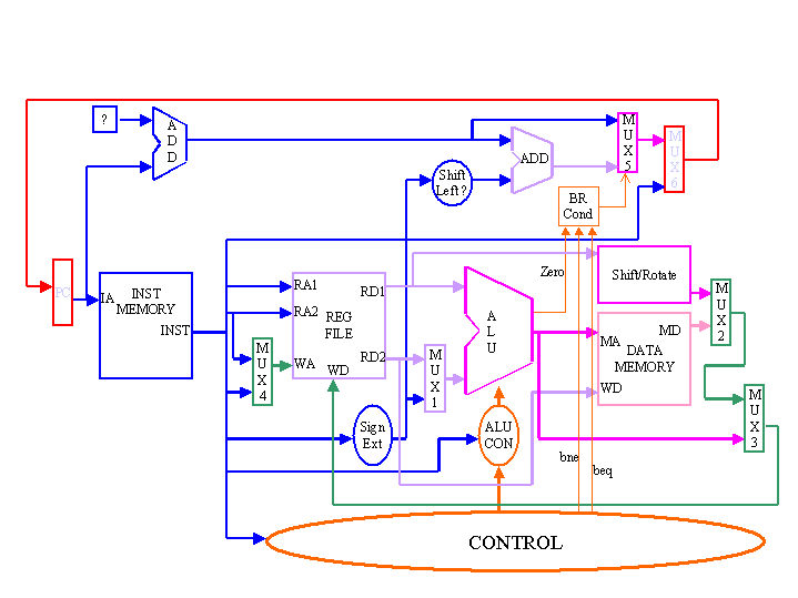
In this lab we will design a control unit for a micro-controller shown below. Here is a brief description of the instructions.
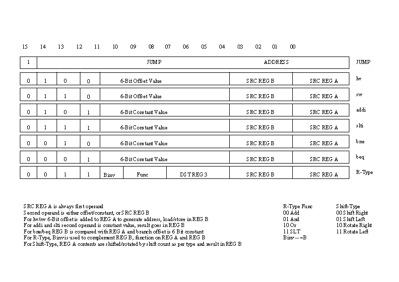
1. Jump: Bit 15=1. Bits 00-14 specify a jump address.
2. lw: bits 15-12=0100. REG B <- Memory [(REG A) + 6-bit offset].
3. sw: bits 15-12=0110. Memory [(REG A) + 6-bit offset] <- REG B.
4. addi: bits 15-12=0101. REG B <- REG A + 6-bit constant
5. slti: bits 15-12=0111. REG B <-(REG A < 6-bit constant) ? 1 : 0.
6. bne: bits 15-12=0010. If (REG A != REG B) PC<-PC+6-bit offset.
7. beq: bits 15-12=0001. If (REG A == REG B) PC<-PC+6-bit offset.
8. R-Type: bits 15-12=0011. DST REG 3 <- REG A (Func) REG B
/* Binv==1 complements REG B contents; Add/And/Or/Slt as in class */
/* Binv is carry to the adder in ALU for this class of instructions */
9. S-Type: bits 15-12=0000. REG B <- REG A shifted/rotated by Count
/* A shift/rotate unit is designed to carry out required function */
All constants are sign extended. The data path is also given below. ALUCON unit will send a 3-bit control signal to ALU. The ALU can perform ADD, AND, and OR operations. The second input of ALU is selected as not-complemented or complemented based on the most-significant bit of the control signal. The remaining two-bits are used to decide which output to select, AND (00), OR (01), ADD/SUB (10) and SLT (11) (SLT output is 1 or 0 depending on if first operand is less than second operand or not). ALUCON unit receives two bits from CONTROL unit and performs the following operation: ADD if the inputs are 00: SUB if the inputs are 01; function specified by IR bits (Binv, Func) if the inputs are 10; and produces output as 0..01 or 0..00 if the first operand is less than or not less than the second operand if the input is 11. Based on this information complete the following table describing input to output mapping for ALUCON unit.
|
2-Bit Input |
3-Bit Output |
|
00 |
|
|
01 |
|
|
10 |
|
|
11 |
|
The control unit generates control signals for MUX1 to MUX6, write register file (WRF), Read Memory (RM), Write Memory (WM), bne, beq, and ALU CON (2-bits). Complete the following table for values of these signals and implement the control unit using Verilog and test it.
|
Inst |
MUX1 |
MUX2 |
MUX3 |
MUX4 |
MUX5 |
MUX6 |
WRF |
RM |
WM |
bne |
beq |
ALUCON |
|
JUMP |
|
|
|
|
|
|
|
|
|
|
|
|
|
Lw |
|
|
|
|
|
|
|
|
|
|
|
|
|
Sw |
|
|
|
|
|
|
|
|
|
|
|
|
|
Addi |
|
|
|
|
|
|
|
|
|
|
|
|
|
Slti |
|
|
|
|
|
|
|
|
|
|
|
|
|
Bne |
|
|
|
|
|
|
|
|
|
|
|
|
|
Beq |
|
|
|
|
|
|
|
|
|
|
|
|
|
R-Type |
|
|
|
|
|
|
|
|
|
|
|
|
|
S-Type |
|
|
|
|
|
|
|
|
|
|
|
|
The following diagrams are given for your reference to the use of multiplexers and the positions of fields. MUX1 is connected to the second input of ALU, MUX2 to input of MUX3, MUX3 to WD (write date) of register file, MUX4 to WA (write address) of register file, MUX5 to the input of MUX6, MUX6 to the input of PC.
In the instruction format, the offset is bit 11-6, the binv is bit 11, and the function code is bit 10-9.